- 您现在的位置:买卖IC网 > Sheet目录323 > DS3050W-100# (Maxim Integrated)IC NVSRAM 4MBIT 100NS 256BGA
3.3V Single-Piece 4Mb Nonvolatile SRAM
with Clock
SRAM Read Mode
The DS3050W executes an SRAM read cycle whenever
CS (RTC chip select) and WE (write enable) are inactive
(high) and CE (SRAM chip enable) is active (low). The
unique address specified by the 19 address inputs (A0
to A18) defines which of the 524,288 bytes of SRAM data
is to be accessed. Valid data will be available to the
eight data output drivers within t ACC (access time) after
the last address input signal is stable, providing that CE
and OE (output enable) access times are also satisfied.
If CE and OE access times are not satisfied, then data
access must be measured from the later occurring sig-
nal ( CE or OE ) and the limiting parameter is either t CO for
CE or t OE for OE rather than address access.
SRAM Write Mode
The DS3050W executes an SRAM write cycle whenever
CS is inactive (high) and the CE and WE signals are
active (low) after address inputs are stable. The later-
occurring falling edge of CE or WE determines the start of
the write cycle. The write cycle is terminated by the earlier
rising edge of CE or WE . All address inputs must be kept
valid throughout the write cycle. WE must return to the
high state for a minimum recovery time (t WR ) before
another cycle can be initiated. The CS and OE control
signal should be kept inactive (high) during SRAM write
cycles to avoid bus contention. However, if the output dri-
vers have been enabled ( CE and OE active) then WE dis-
ables the outputs in t ODW from its falling edge.
Clock Operations
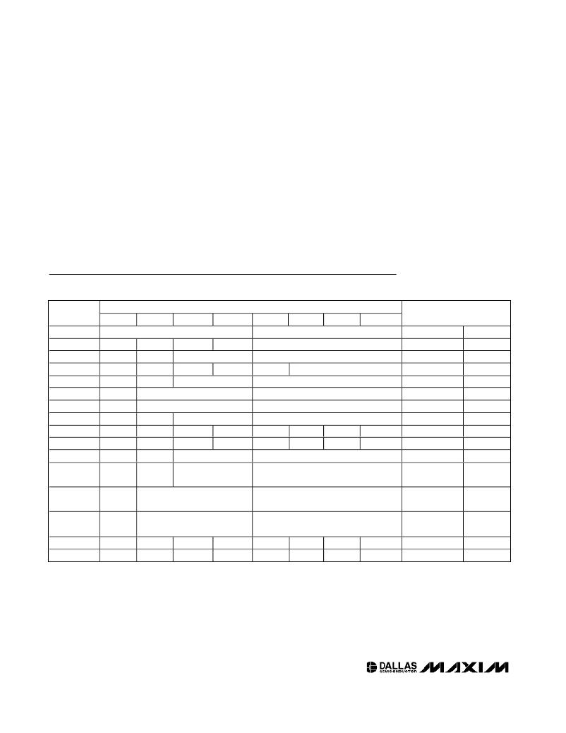
Table 2. RTC Register Map
ADDRESS
B7
B6
B5
B4
DATA
B3
B2
B1
B0
FUNCTION/RANGE
xxxxFh
10 YEAR
YEAR
YEAR
00 – 99
xxxxEh
xxxxDh
X
X
X
X
X
10 M
10 DATE
MONTH
DATE
MONTH
DATE
01 – 12
01 – 31
xxxxCh
xxxxBh
X
X
FT
X
X
10 HOUR
X
X
DAY
HOUR
DAY
HOUR
01 – 07
00 – 23
xxxxAh
xxxx9h
X
OSC
10 MINUTES
10 SECONDS
MINUTES
SECONDS
MINUTES
SECONDS
00 – 59
00 – 59
xxxx8h
W
R
10 CENTURY
CENTURY
CONTROL
00 – 39
xxxx7h
xxxx6h
WDS
AE
BMB4
Y
BMB3
ABE
BMB2
Y
BMB1
Y
BMB0
Y
RB1
Y
RB0
Y
WATCHDOG
INTERRUPTS
?
?
xxxx5h
xxxx4h
xxxx3h
xxxx2h
AM4
AM3
AM2
AM1
Y
Y
10 DATE
10 HOURS
10 MINUTES
10 SECONDS
DATE
HOURS
MINUTES
SECONDS
ALARM DATE
ALARM
HOURS
ALARM
MINUTES
ALARM
SECONDS
01 – 31
00 – 23
00 – 59
00 – 59
xxxx1h
xxxx0h
Y
WF
Y
AF
Y
0
Y
BLF
Y
0
Y
0
Y
0
Y
0
UNUSED
FLAGS
?
?
x = Don’t care address bits.
X = Unused. Read/writeable under write and read bit control.
FT = Frequency test bit.
OSC = Oscillator start/stop bit.
W = Write bit.
R = Read bit.
WDS = Watchdog steering bit.
BMB0–BMB4 = Watchdog multiplier bits.
RB0, RB1 = Watchdog resolution bits.
AE = Alarm flag enable.
Y = Unused. Read/writeable without write and read bit control.
ABE = Alarm in backup mode enable.
AM1–AM4 = Alarm mask bits.
WF = Watchdog flag.
AF = Alarm flag.
0 = Reads as a 0 and cannot be changed.
BLF = Battery low flag.
12
____________________________________________________________________
发布紧急采购,3分钟左右您将得到回复。
相关PDF资料
DS3065W-100#
IC NVSRAM 8MBIT 100NS 256BGA
DS3065WP-100IND+
IC SRAM 3.3V 8MB 34POWERCAP MOD
DS3070W-100#
IC NVSRAM 16MBIT 100NS 256BGA
DS321X
KIT X-WIDE DESIGN STRIP VERT
DS323X
KIT X-WIDE DESIGN STRIP VERT
DS87001-E52
ADAPTER MCU 52-TQFP TO 40-DIP
DS89C450-K00
EVAL KIT FOR DS89C450
DSP56311EVM
KIT EVALUATION FOR DSP56311
相关代理商/技术参数
DS30519
制造商:DIODES 制造商全称:Diodes Incorporated 功能描述:2.0A SURFACE MOUNT SCHOTTKY BARRIER RECTIFIER
DS305710A
制造商:Amphenol Corporation 功能描述:
DS305710A(621)
制造商:Amphenol Corporation 功能描述:
DS305712A
制造商:Amphenol Corporation 功能描述:
DS305712A(621)
制造商:Amphenol Corporation 功能描述:
DS305716A
制造商:Amphenol Corporation 功能描述:
DS305716A621
制造商:Amphenol Corporation 功能描述:
DS30574A
制造商:Amphenol Corporation 功能描述:
